As the energy constraint becomes increasingly evident, the solar PV power generation system attracts growing attention. The direct current generated by solar cells and wind-powered generators should be inverted by inverters before being combined to the grid. Therefore, the design of solar on grid inverters determines whether the solar PV system will operate reasonably, efficiently, and economically.
- Structure Principle of Solar On Grid Inverter
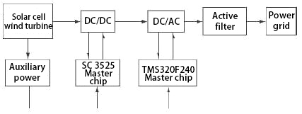
The structure of solar grid tie inverter is presented in the following diagram, consisting of front-end DC/DC inverters and back-end DC/AC inverters. The basic principle is that low-voltage direct current is converted into high-voltage direct current through the high-frequency conversion technology and passes the power-frequency inverter circuit to be converted into 220V alternating current. Such a structure has the merits of a simple circuit, a small loss from a no-load inverter power supply, a large output power, a high inversion efficiency, high stability, and slight distortion.
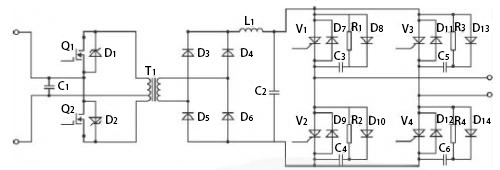
The main circuit of solar on grid inverter is presented in the following diagram. The double-ended output SPWM chip controlled by the DC/DC module generates PWM waveforms with a variable duty ratio to drive the polarity of the thyristor that controls connection and disconnection and to eventually control the output waveform.
- DC/DC Control Modules of Solar Grid Tie Inverters
The PWM control chip is exclusively applied to driving the MOSFET of P-channel power. The main control chip's output drive is pull-and-push output and can directly drive the MOS transistor. It consists of an under-voltage locking circuit, a soft-start control circuit, PWM latches. Apart from over-current protection and frequency adjustment, it restricts the maximum duty ratio. Two outputs are connected to two MOS transistors to control connection and disconnection. To raise the effective control of the pull-and-push DC/DC high-frequency boost and raise the accuracy of the high-frequency modulation, there is a detection circuit is designed for inverter, to detect the output current and voltage and feedback them to the control chip.
- DC/AC Control Modules of Solar On Grid Inverters
Voltage and Current Detection Circuits of Grid On Inverters
(1) Zero-crossing Detection Circuit for Network Voltages
The AC current converted by the solar inverter should have an identical voltage and frequency to those of the power grid before being connected. Hence the output voltage should undergo phase-locked control. The output voltage sends signals through sine waves, while the control chip can only identify TTL level signals. It is necessary to convert the sine-wave signals of one circuit to TTL level signals. If the voltage of the grid to be detected exceeds zero, the circuit will output high electric levels. The zero-crossing detection circuit of the power grid is presented in the following diagram.
Square signals received by the power grid's zero-crossing detection circuit are transmitted to the capture pin of the DSP chip through the Schmitt inverting circuit. Then the capture unit triggers disconnection and starts the phase lock after detecting the increase.
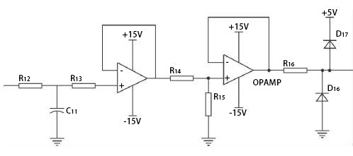
(2) AC Detection Circuit
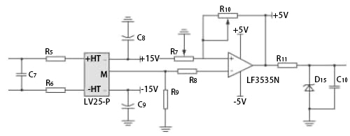
The AC detection circuit uses a closed-loop current sensor, as is shown in the following diagram. The alternating current is measured in electric isolation according to the Hall Closed-loop Principle. When the alternating current passes the sensor, the sensor converts electric signals into voltage signals and sends them to the signal processing circuit. Once processed, these signals are transmitted into the pin of the DSP chip. The processing circuit is composed of the RC filter circuit and two groups of integrated OPA isolation circuits.
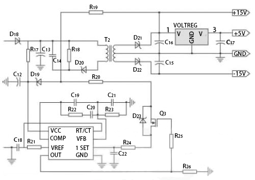
The control circuit, signal gathering circuit, and the switching tube drive circuit of solar on grid inverters need different adaptive power supplies. Thus an independent power supply should be provided for powering these circuits. The voltages of the designed auxiliary power supplies include +15V, -15V, and +5V. A single-ended flyback DC/DC topographical structure is adopted, with stable and reliable operation. The basic circuit of the auxiliary power supply is listed in the following diagram.