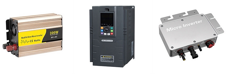
In photovoltaic power generation, energy storage systems, industrial automation, motor drives, and UPS applications, the inverter plays a central role in converting DC power into AC power. Whether it is a grid-connected solar inverter, an energy storage hybrid inverter, an industrial frequency inverter, or a high-power three-phase inverter, high-speed switching inevitably generates electromagnetic interference (EMI).
As power density and switching frequency continue to increase, EMI has become a key factor affecting product stability and international compliance certification. Inverter.com holds the view that systematically controlling electromagnetic interference during the design phase is therefore one of the core capabilities in developing high-quality inverters.
Why Do Inverters Generate Electromagnetic Interference?
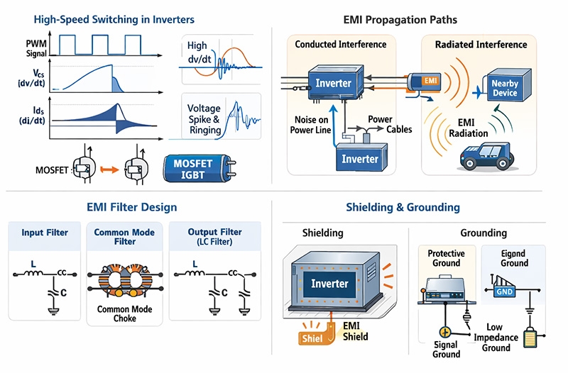
The root cause of EMI in inverters lies in the high-speed switching behavior of power devices. Modern inverters widely use PWM modulation technology. By rapidly turning MOSFETs, IGBTs, or SiC devices on and off, the inverter generates an output voltage close to a sine wave. During this process, the voltage slew rate (dv/dt) and current slew rate (di/dt) are extremely high, with transitions completed in very short time intervals. These rapid changes excite parasitic inductance and parasitic capacitance in the circuit, resulting in voltage spikes and high-frequency oscillations.
High-frequency energy then propagates outward through power lines (conducted emission) or radiates into surrounding space (radiated emission). In high-voltage, high-current power inverters or three-phase systems, interference is often more pronounced due to higher DC bus voltage and concentrated energy.
From the perspective of interference modes, inverter EMI can be divided into: Differential-mode interference, which exists between phase conductors, and common-mode interference, which exists between phase conductors and ground. In grid-connected solar inverters or high-power three-phase inverters, common-mode interference is often the main reason for EMC test failures. Parasitic capacitance between switching nodes and ground can generate high-frequency leakage currents, which are difficult to suppress without proper design.
EMI Propagation Paths in Inverter Systems
Electromagnetic interference in inverter systems mainly spreads in 2 ways:
- Conducted Interference: Conducted interference propagates through conductors such as power cables and signal lines. Rapid current changes produced by switching devices create voltage fluctuations on power and signal lines. These fluctuations travel along connected wiring and disturb other equipment.
- Radiated Interference: Radiated interference spreads in the form of electromagnetic waves. Switching devices and PCB layouts generate alternating electromagnetic fields that radiate into the surrounding space. Any nearby equipment within this field may experience interference.
Methods to Reduce Electromagnetic Interference in Inverters
● Optimize Circuit Design
- Select Appropriate Switching Devices: Different switching devices exhibit different switching characteristics and EMI performance. In the context of a frequency inverter, MOSFETs offer fast switching speed but typically have higher on-resistance. IGBTs combine fast switching capability with lower conduction voltage drop. When selecting switching devices, designers must balance switching speed, conduction loss, and turn-off loss according to the specific application. Choosing devices with controlled switching characteristics can effectively reduce EMI generation.
- Optimize Switching Frequency: Higher switching frequency reduces output voltage THD, but it also increases EMI. Design requires a practical trade-off between output waveform quality and electromagnetic interference. Through simulation and experimental validation, an optimal switching frequency can be selected that meets voltage quality requirements while keeping EMI within acceptable limits.
- Adopt Soft-Switching Techniques: Soft-switching is an effective method for reducing inverter EMI. Unlike hard switching, soft-switching introduces resonant circuits so that switching occurs at zero voltage or zero current. This significantly reduces dv/dt and di/dt during transitions, thereby lowering EMI. Common soft-switching techniques include Zero Voltage Switching (ZVS) and Zero Current Switching (ZCS).
● Strengthen Filter Design
- Input Filter: Installing an input filter at the inverter’s DC side suppresses EMI from the power source and prevents inverter-generated noise from feeding back into the supply. Input filters typically consist of inductors and capacitors designed to attenuate specific frequency ranges.
- Output Filter: The output filter reduces harmonic components in the inverter output voltage and minimizes interference to the load. LC filters are commonly used to smooth the output voltage and reduce high-frequency noise.
- Common-Mode Filter: Common-mode interference is widespread in inverter systems and often couples through capacitance between lines and ground. A common-mode filter usually consists of a common-mode choke and high-frequency capacitors. The choke presents high impedance to common-mode signals, while capacitors provide a low-impedance path to ground, effectively bypassing high-frequency noise.
● Improve PCB Layout and Routing
- Proper Component Placement: High-EMI components, such as switching devices, inductors, and capacitors, should be grouped and kept away from sensitive circuits, such as control and signal processing sections. Input and output circuits should be physically separated to reduce mutual interference.
- Optimize Routing: Routing significantly impacts EMI performance. Minimize the length of high-frequency signal traces. Reduce loop area to lower radiated emissions. Use wide and short traces for power and ground to reduce resistance and inductance. Consider multilayer PCB designs with dedicated power and ground planes to enhance electromagnetic interference (EMI) immunity.
● Shielding and Grounding
- Shielding: Metal enclosures can effectively reduce radiated interference by confining EMI within the inverter housing and blocking external electromagnetic disturbances. Shield continuity and structural integrity are critical. Gaps or openings may allow EMI leakage.
- Grounding: Proper grounding is essential for EMI control. The grounding system typically includes: Protective grounding for safety, connecting conductive enclosures to earth. Signal grounding to provide a stable reference potential. Ground resistance must be kept low, and ground loops should be carefully avoided to prevent unwanted voltage drops and interference coupling.
Conclusion
Reducing electromagnetic interference in inverters is a systematic engineering task. It requires coordinated optimization of circuit design, filtering, PCB layout, shielding, and grounding. By carefully selecting switching devices, optimizing switching frequency, adopting soft-switching techniques, strengthening filter design, improving PCB layout, and implementing proper shielding and grounding, inverter-generated EMI can be effectively reduced. This improves performance, reliability, and compliance with international EMC standards, ensuring stable operation of the entire power electronics system. In practical applications, these methods should be flexibly applied according to the inverter’s specific requirements to achieve optimal electromagnetic compatibility.
If you are planning a photovoltaic system, energy storage project, or industrial automation solution, you may explore our solar inverter, hybrid inverter, frequency inverter, and three-phase inverter product series. These solutions are designed with EMC considerations from the outset, providing stable, reliable, and standards-compliant power conversion for your system.